- 您现在的位置:买卖IC网 > Sheet目录961 > AS1115 DB-YELLOW (ams)BOARD DEMO AS1115 YELLOW
�� �
�
�AS1115�
�Datasheet� -� D� e� t� a� i� l� e� d� D� e� s� c� r� i� p� t� i� o� n�
�I2C� Interface�
�The� AS1115� supports� the� I2C� serial� bus� and� data� transmission� protocol� in� high-speed� mode� at� 3.4MHz.� The� AS1115� operates� as� a� slave� on� the�
�I2C� bus.� The� bus� must� be� controlled� by� a� master� device� that� generates� the� serial� clock� (SCL),� controls� the� bus� access,� and� generates� the� START�
�and� STOP� conditions.� Connections� to� the� bus� are� made� via� the� open-drain� I/O� pins� SCL� and� SDA.�
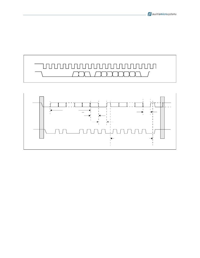
�Figure� 18.� I2C� Interface� Initialization�
�1�
�8�
�9�
�1�
�8�
�9�
�0�
�0�
�0�
�0�
�0�
�A1�
�A0� R/W�
�D15� D14� D13� D12� D11� D10�
�D9�
�D8�
�Default values at power up: A1 = A0 = 0�
�Figure� 19.� Bus� Protocol�
�SDI�
�MSB�
�Slave Address�
�R/W�
�Direction� Bit�
�ACK� from�
�Receiver�
�ACK� from�
�Receiver�
�SCL�
�1�
�2�
�6�
�7�
�8�
�9�
�1�
�2�
�3-8�
�8�
�9�
�START�
�ACK�
�ACK�
�Repeat if More Bytes Transferred�
�STOP� or�
�Repeated�
�START�
�The� bus� protocol� (as� shown� in� Figure� 19� )� is� defined� as:�
�-� Data� transfer� may� be� initiated� only� when� the� bus� is� not� busy.�
�-� During� data� transfer,� the� data� line� must� remain� stable� whenever� the� clock� line� is� HIGH.� Changes� in� the� data� line� while� the� clock� line� is�
�HIGH� will� be� interpreted� as� control� signals.�
�The� bus� conditions� are� defined� as:�
�-�
�-�
�-�
�-�
�Bus� Not� Busy� .� Data� and� clock� lines� remain� HIGH.�
�Start� Data� Transfer� .� A� change� in� the� state� of� the� data� line,� from� HIGH� to� LOW,� while� the� clock� is� HIGH,� defines� a� START� condition.�
�Stop� Data� Transfe� r.� A� change� in� the� state� of� the� data� line,� from� LOW� to� HIGH,� while� the� clock� line� is� HIGH,� defines� the� STOP� condition.�
�Data� Valid� .� The� state� of� the� data� line� represents� valid� data,� when,� after� a� START� condition,� the� data� line� is� stable� for� the� duration� of� the�
�HIGH� period� of� the� clock� signal.� There� is� one� clock� pulse� per� bit� of� data.�
�Each� data� transfer� is� initiated� with� a� START� condition� and� terminated� with� a� STOP� condition.� The� number� of� data� bytes� transferred�
�between� START� and� STOP� conditions� is� not� limited� and� is� determined� by� the� master� device.� The� information� is� transferred� byte-wise� and�
�each� receiver� acknowledges� with� a� ninth-bit.�
�Within� the� I2C� bus� specifications� a� high-speed� mode� (3.4MHz� clock� rate)� is� defined.�
�-� Acknowledge� :� Each� receiving� device,� when� addressed,� is� obliged� to� generate� an� acknowledge� after� the� reception� of� each� byte.� The� mas-�
�ter� device� must� generate� an� extra� clock� pulse� that� is� associated� with� this� acknowledge� bit.� A� device� that� acknowledges� must� pull� down� the�
�SDA� line� during� the� acknowledge� clock� pulse� in� such� a� way� that� the� SDA� line� is� stable� LOW� during� the� HIGH� period� of� the� acknowledge�
�clock� pulse.� Of� course,� setup� and� hold� times� must� be� taken� into� account.� A� master� must� signal� an� end� of� data� to� the� slave� by� not� generat-�
��Revision� 1.08�
�9� -� 25�
�发布紧急采购,3分钟左右您将得到回复。
相关PDF资料
AS1116 DB-YELLOW
BOARD DEMO AS1116 YELLOW
AS3691A EB
BOARD EVAL AS3691A
AS5030 DB
BOARD DEMO AS5030
AS5048-DB-1.0
BOARD DEMO AS5048
AS5215 DB
BOARD DEMO AS5215
AS5245 DB
BOARD DEMO AS5245
AS5304-DK-1.0
BOARD DEMO AS5304
AS5311 DB
BOARD EVAL FOR AS5311
相关代理商/技术参数
AS1115 WG DB
制造商:ams 功能描述:Demo Board Whitegood
AS1115 WHITE GOOD DB
功能描述:DEMOBOARD EVAL WHITE GOOD RoHS:否 类别:编程器,开发系统 >> 评估演示板和套件 系列:- 标准包装:1 系列:PSoC® 主要目的:电源管理,热管理 嵌入式:- 已用 IC / 零件:- 主要属性:- 次要属性:- 已供物品:板,CD,电源
AS11150FLF
制造商:TT Electronics / IRC 功能描述:AS11150FLF
AS11150HLF
制造商:TT Electronics / IRC 功能描述:AS11150HLF
AS11150JLF
制造商:TT Electronics / IRC 功能描述:AS11150JLF
AS11151FLF
制造商:TT Electronics / IRC 功能描述:AS11151FLF
AS11151HLF
制造商:TT Electronics / IRC 功能描述:AS11151HLF
AS11151JLF
制造商:TT Electronics / IRC 功能描述:AS11151JLF